Advanced Search
Keyword
By photographer
Category
All
3D Renders
Animals
Constructions
Graphics
Industrial
Nature
Objects
People
Seasonal
Textures
Transportation
Shape
Any
Portrait
Landscape
Square
Date
All time
Last day
Last week
Last month
Last year
License
All License
Non-Commercial
Commercial
Creative Commons - CC0
Color
Photos
Latest Photos
Most Popular Photos
Most Downloaded Photos
Most Loved Photos
Featured Photos
Popular Keywords
Collections
Categories
Animals
Birds
Bones
Cats and Dogs
Fish
Insects
Reptiles
Transportation
Airplanes
Automobile
Bikes
Boats
Trains
Graphics
Clip Art
Logo Templates
Photoshop Brushes
Vector
Web Templates
Constructions
Abandoned
Bridges
Castle
Church & Cemetery
Glass & Windows
Office & Workspace
Roads & Streets
Skyscrapers
Stairs & Ladders
Tanks & Towers
Tunnels
Vents & Drains
Nature
Fire, Fog & Smoke
Flowers
Ice & Snow
Landscape
Lunar & Space
Plants & Trees
Sea & Water
Sky & Clouds
Stone & Rocks
Industrial
Electricity
Locks & Chains
Pipes & Wire
Rusted
Screws, Bolts & Wheels
Objects
Art Supplies
Cosmetics
Electronics
Entertainment
Flags
Food & Drink
Furniture
Household Items
Jewelry
Medical
Money
Music
Office Supplies
Paper & Books
Religion
Sculptures
Signs
Stamps
Tools & Weapons
Toys
People
Children
Human Activity
Human Bones
Human Closeups
Portraits
Sports Activity
Seasonal
Christmas
Easter
Fireworks
Halloween
Valentines Day
3D Renders
3D Landscapes
3D Text
Abstract Shapes
Boxes and Models
Textures
Burned Textures
Dirt & Mud Textures
Fabric Textures
Grunge Textures
Light Effects
Metal & Rust
Misc Textures
Organic Textures
Paint Textures
Paper Textures
Plastic Textures
Stone & Rock Textures
Water & Liquid Textures
Wood Textures
Blog
Premium
Stock Photos
Stock Vectors
Stock Footage
Info
About us
Advertise
Contact
Terms of Use
FAQs
Tutorials
Resources
Latest Comments
Upload a Photo
Login
Register
3
Notifications
Icon Freebie:
Download a camera icon set for free!
Feb 10th 2022
On the Blog:
Free Educational Illustration Resources
Feb 10th 2022
Creator Spotlight:
12 Free Stock Images & Illustrations by Jack Moreh
Feb 10th 2022
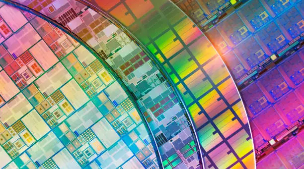
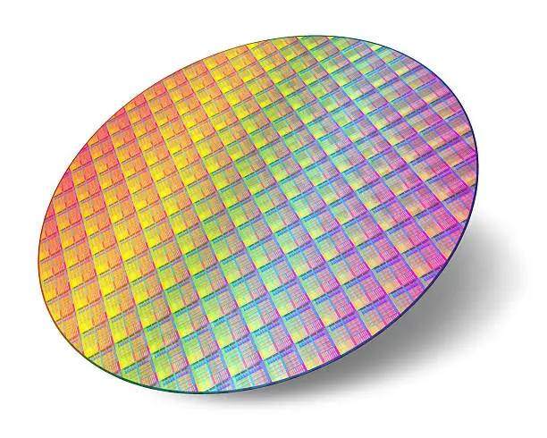
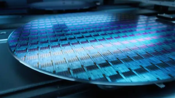
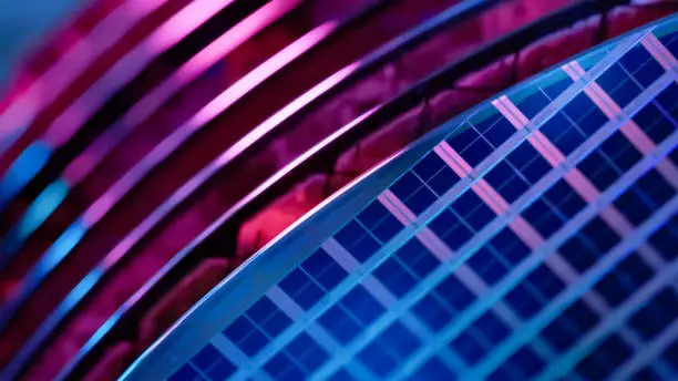
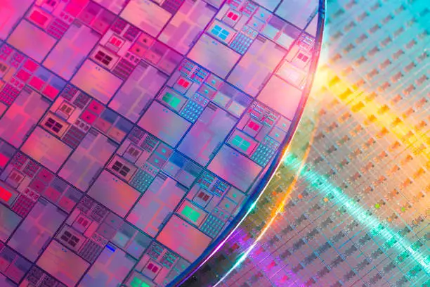
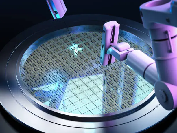
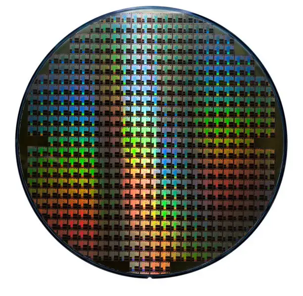
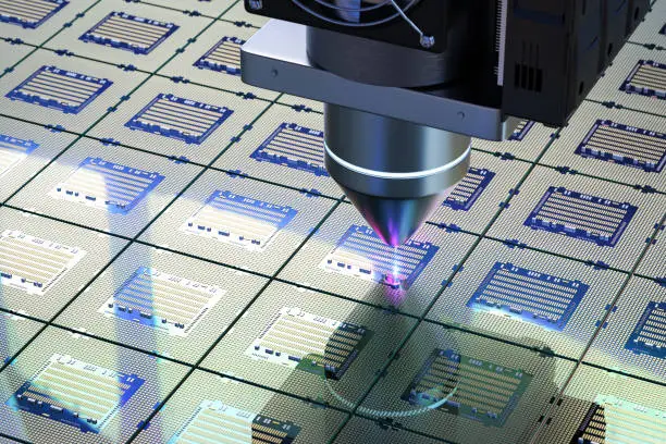
wafer
Stock Photos
Premium Photos & Textures.
Search
"wafer"
Search
Get 15% off iStock with code: STOCKVAULT15 →
Free Photos
Premium Photos
Premium Vectors
Premium Footage
Premium Photos
Premium Vectors
Premium Footage